13691652059
sujunisme@126.com
中文
EN
产品中心
品牌
询价
资讯
本地
关于我们
企业文化
公司介绍
联系我们
联系我们
取消
首页
产品中心
品牌
询价
资讯
关于我们
联系我们
中文
EN
电阻器(1464842)
电容器(1233524)
电感器、线圈、扼流圈(160301)
电位器、可变电阻器(31938)
變壓器(15404)
晶体、振荡器、谐振器(755151)
分立半导体产品(252065)
传感器、变换器(174312)
集成电路 (IC)(656537)
射频和无线(109622)
芯向中国 科创世界
一体化制造 助力芯成长
芯向中国 科创世界
一体化制造 助力芯成长
Previous
Next
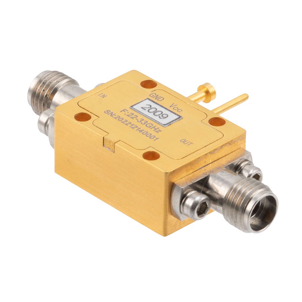
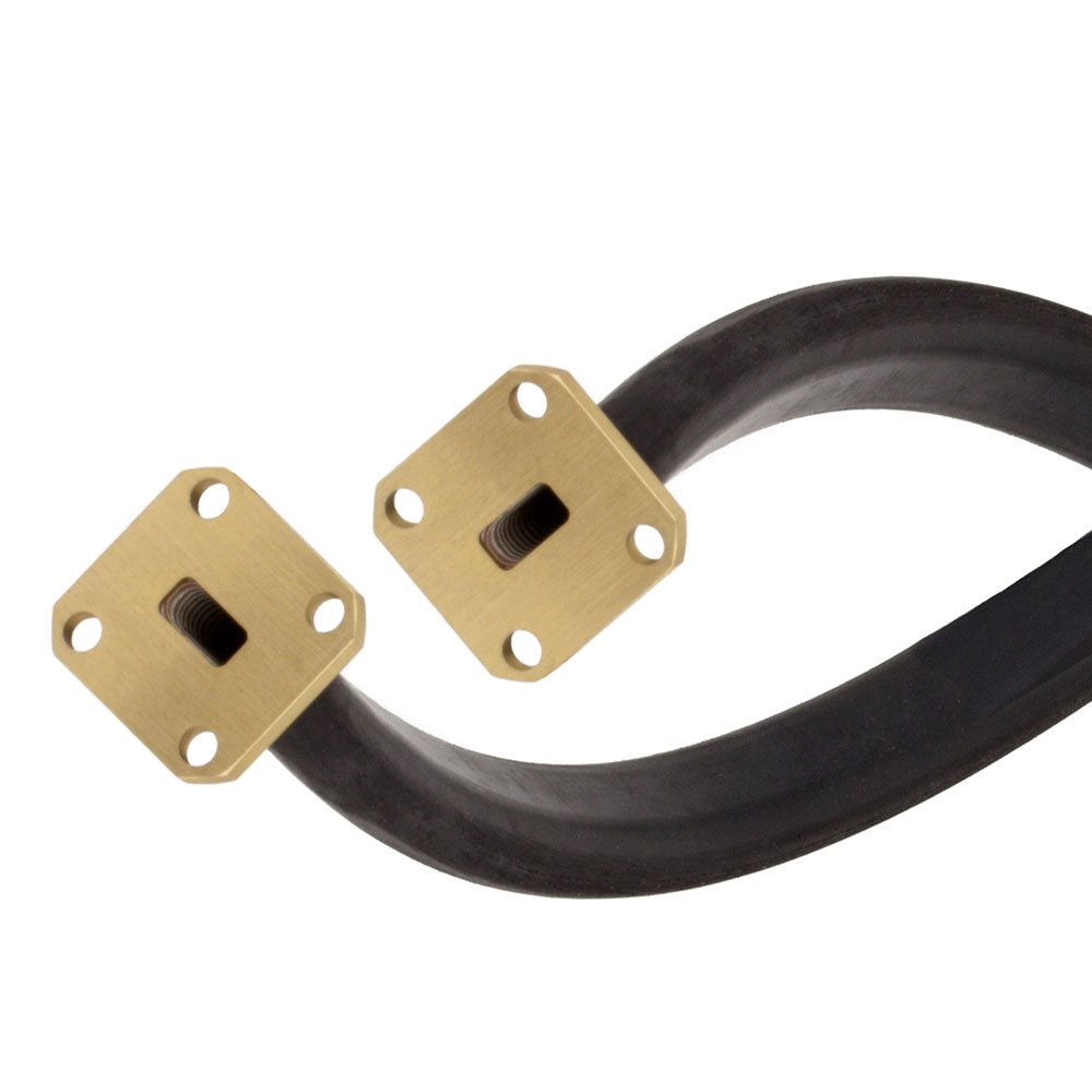
FM82P2009"
Fairview Microwave
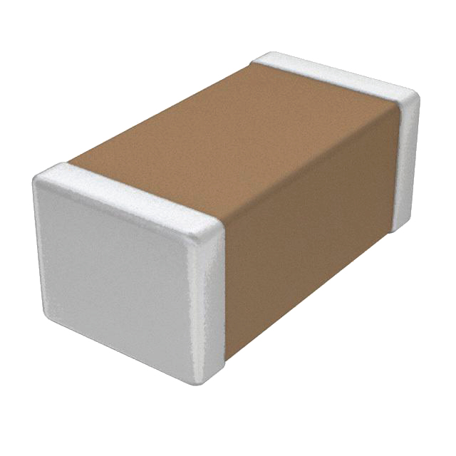
CHV1812N250333JCT"
Cal-Chip Electronics, Inc.
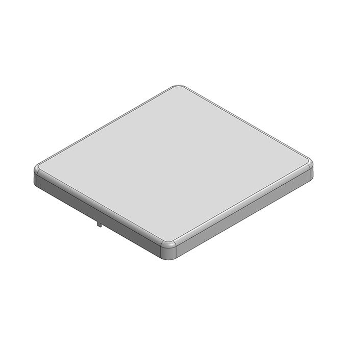
MS366-10S-NS"
Masach
CHV1812N2K0102JCT"
Cal-Chip Electronics, Inc.
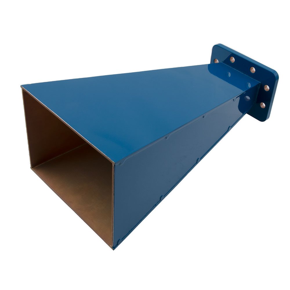
FM9861B-15-CPRG"
Fairview Microwave
CHV1812N1K0122JCT"
Cal-Chip Electronics, Inc.
SA18N5WA-06"
Fairview Microwave
FMSW6450"
Fairview Microwave
FM82P2009
PHASE SHIFTER 2.92MM 33 GHZ
Fairview Microwave
详情
CHV1812N250333JCT
HVCAP1812 COG .033UF 5% 250V
Cal-Chip Electronics, Inc.
详情
MS366-10S-NS
36.6X34.1X3.3 MM RF SHIELD
Masach
详情
CHV1812N2K0102JCT
HVCAP1812 COG 1000PF 5% 2KV
Cal-Chip Electronics, Inc.
详情
FM9861B-15-CPRG
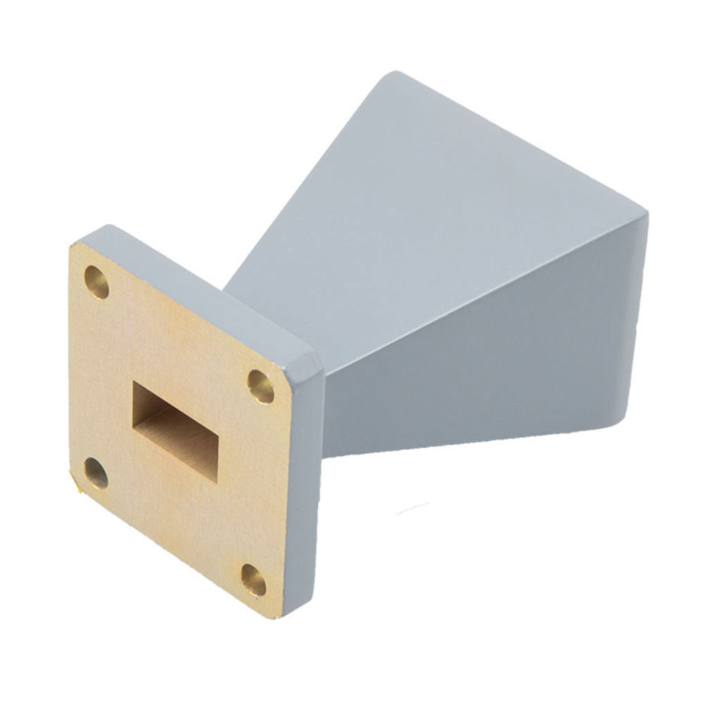
WG ANTENNA WR-187 3.95-5.85 GHZ
Fairview Microwave
详情
CHV1812N1K0122JCT
HVCAP1812 COG 1200PF 5% 1KV
Cal-Chip Electronics, Inc.
详情
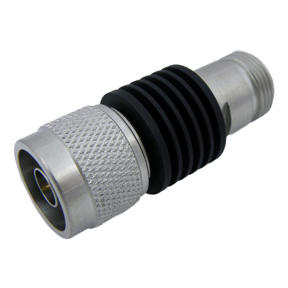
SA18N5WA-06
FXD ATTN PLUG-JACK TYPE N 1.35
Fairview Microwave
详情
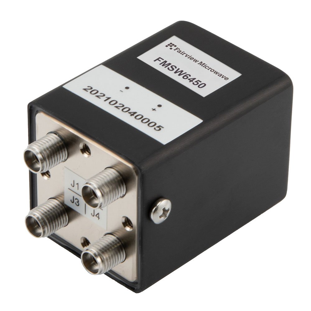
FMSW6450
EM RELAY SWITCH 40 GHZ 28 V 2.92
Fairview Microwave
详情
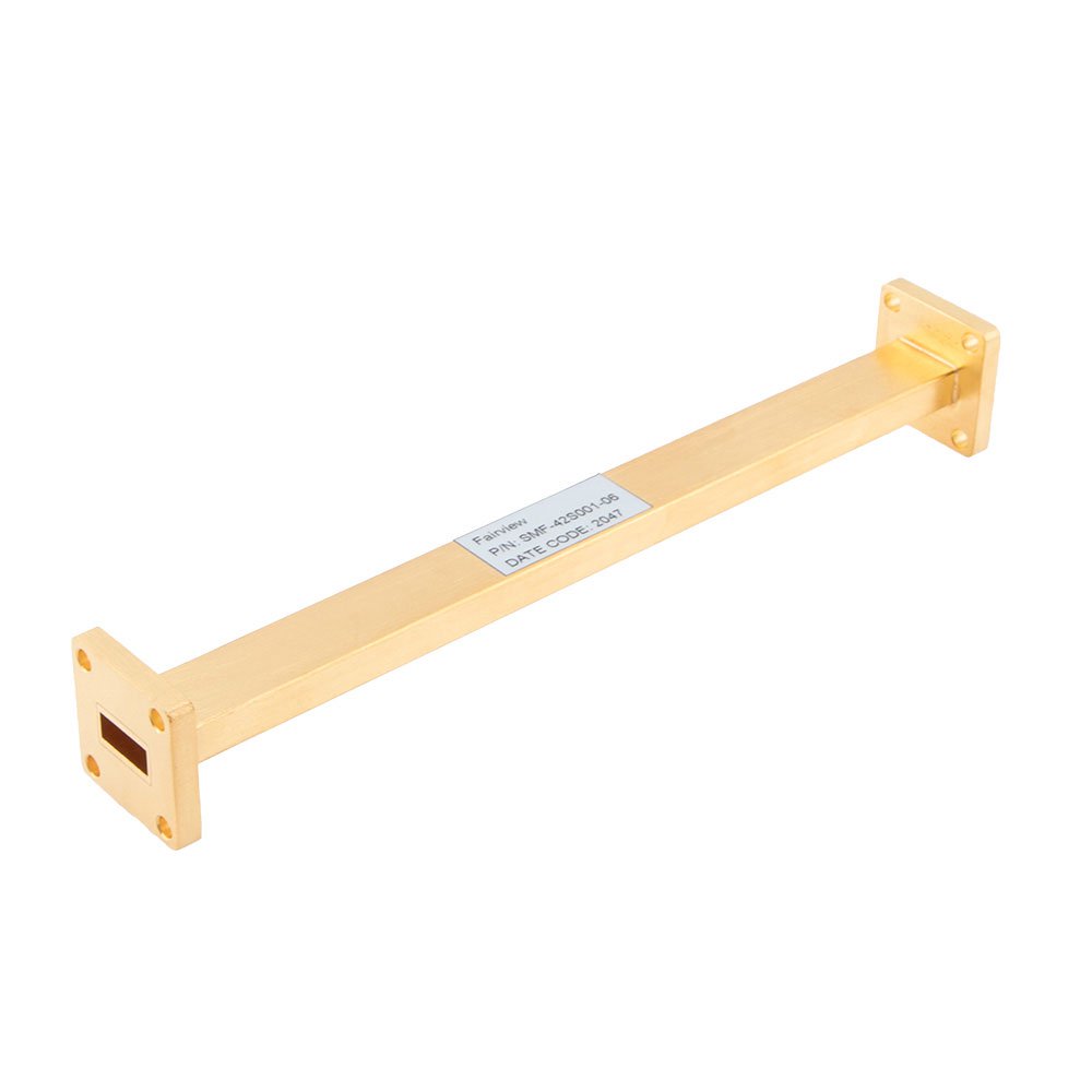
SMF-42S001-06
WAVEGUIDE SEC WR-42 18GHZ-26.5GH
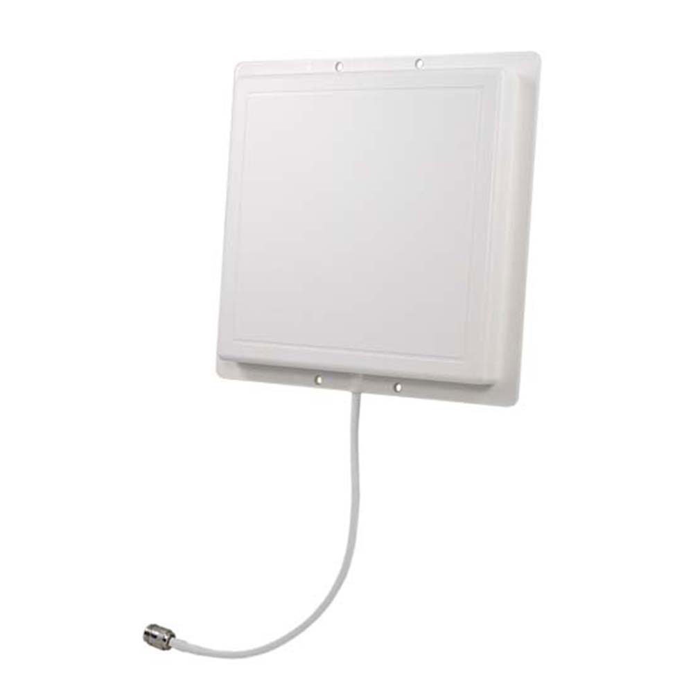
FM51FP1005
TYPE N JACK 900 MHZ 8 DBI FLAT P
SMW28TF005-12
FLEXIBLE WG WR-28 26.5-40 GHZ
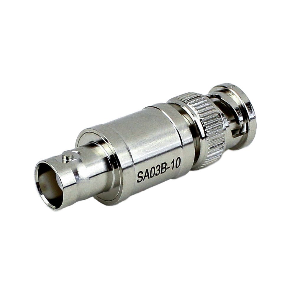
SA03B-10
FXD ATTN PLUG-JACK BNC
MS366-10S-NS
36.6X34.1X3.3 MM RF SHIELD
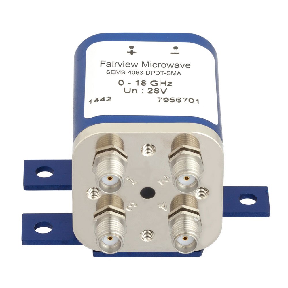
SEMS-4063-DPDT-SMA
EM RELAY SWITCH 18 GHZ 28 V SMA
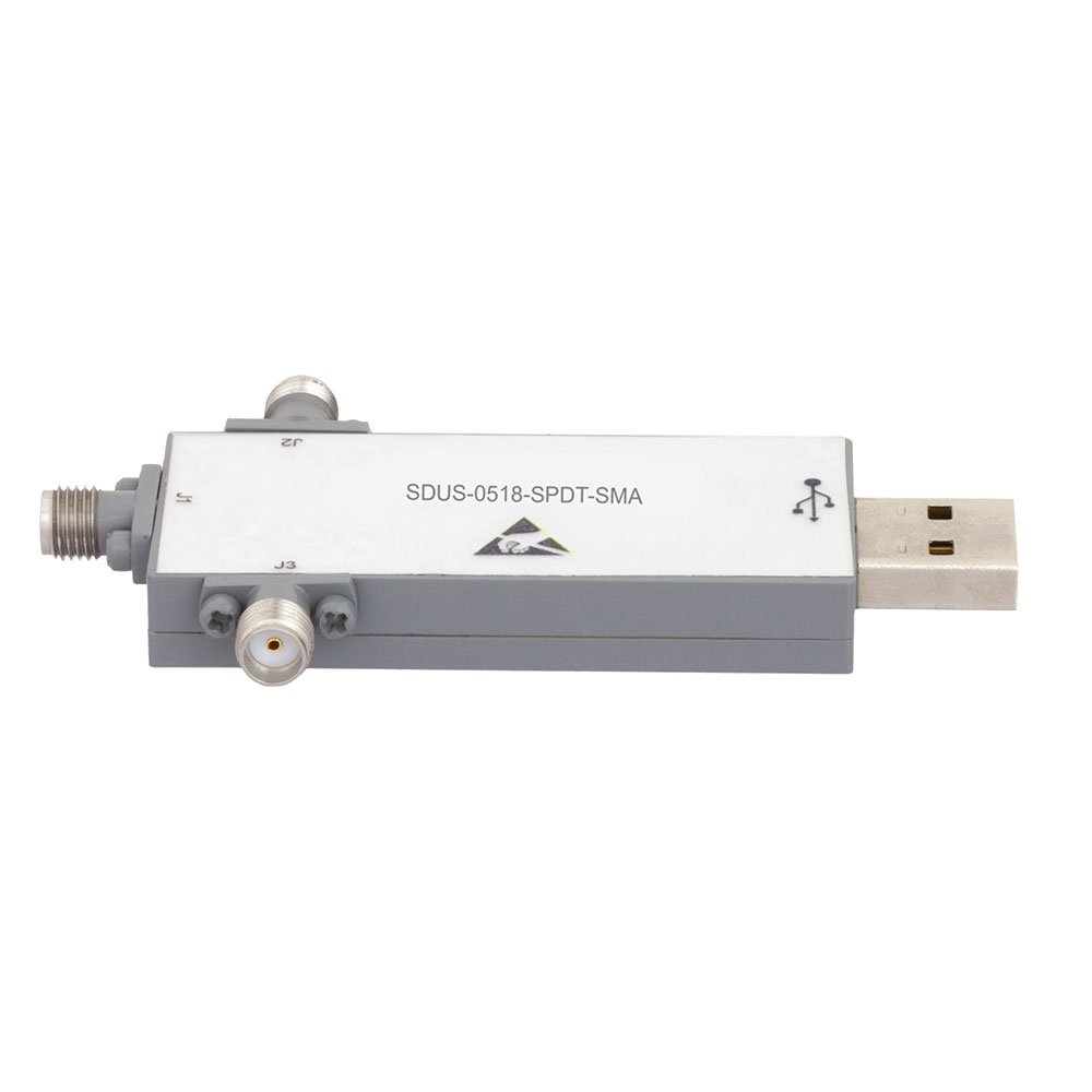
SDUS-0518-SPDT-SMA
HIGH ISO USB SWITCH TYPE SMA 500
CHV1808N500472KXT
HVCAP1808 X7R 4700PF 10% 500V
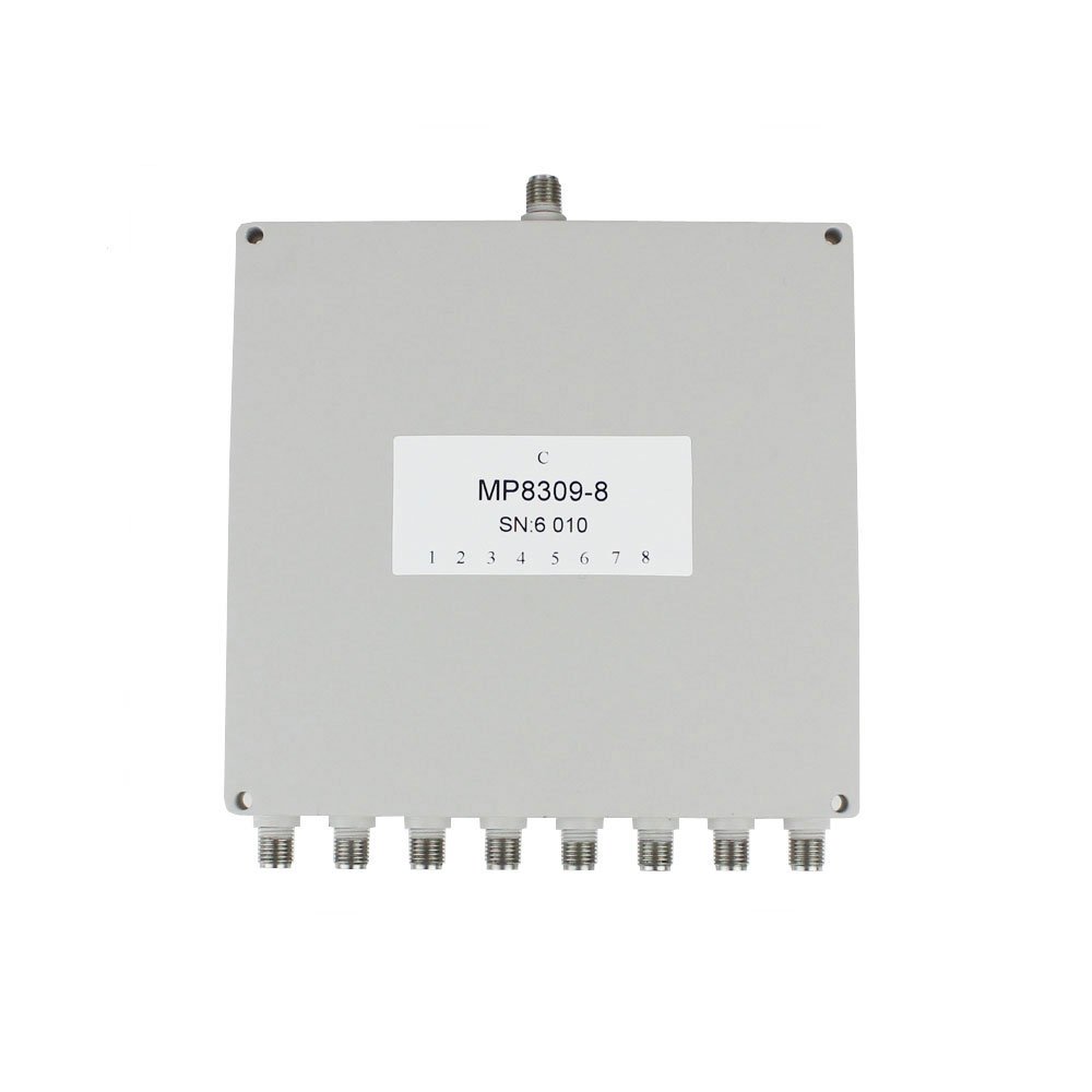
MP8309-8
POWER DIVIDER 2 GHZ SMA
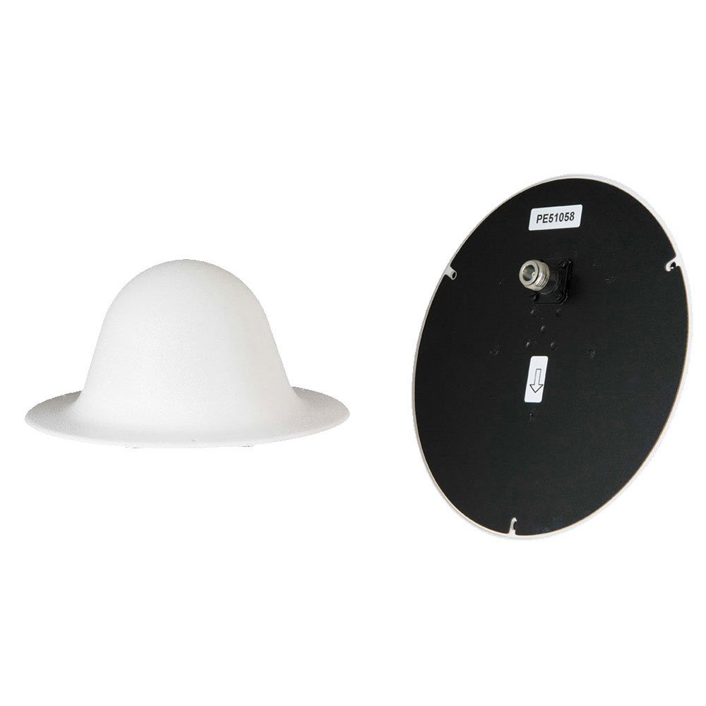
FM51058
ANTENNA TYPE N JACK 800 MHZ-3 GH
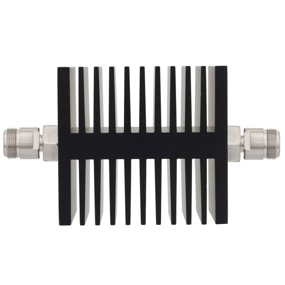
SA18NFNF50W-40
FXD ATTN JACK-JACK TYPE N 1.6
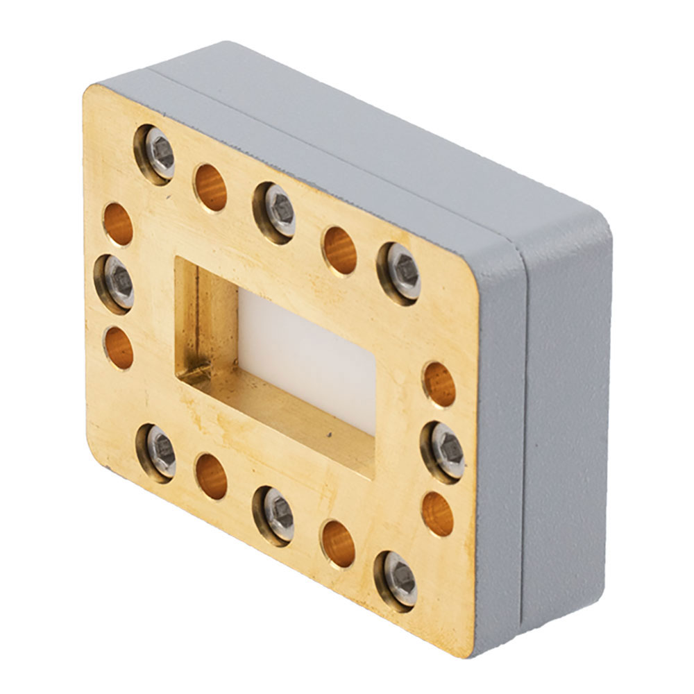
FMWGP1005
WR-137 WAVEGUIDE PRESSURE WINDOW
FMWAN051-15
WG ANTENNA WR-51 15-22 GHZ
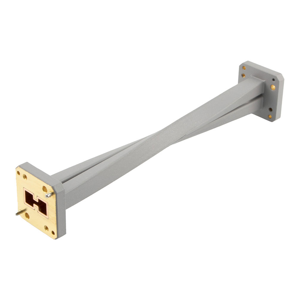
FMWRD650TW1001
WG TWIST WRD-650 6.5-18 GHZ UG
MS366-10F-NS
36.6X34.1X3.3 MM RF FRAME
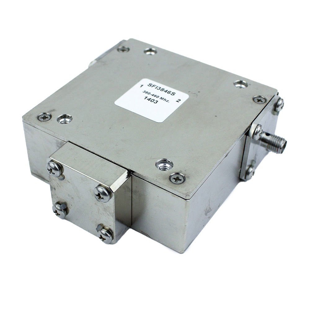
SFI3846S
ISOLATOR SMA JACK 380MHZ-460MHZ1
FMBL1001
20 MHZ TO 520 MHZ BALUN AT 50 OH
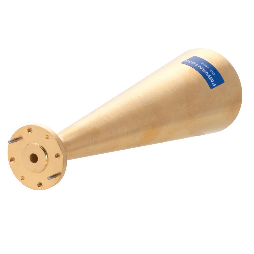
FMWAN1036
WG ANTENNA WR-19 50-58 GHZ
PMDM
agent
YAGEO
agent
EMIT
agent
TE Connectivity AMP Connectors
agent
Wickmann / Littelfuse
agent
3M
agent
Intersil (Renesas Electronics Corporation)
agent
B&K Precision
agent
Comair Rotron
agent
Hirose Electric Co., Ltd.
agent
Visual Communications Company, LLC
agent
Zetex Semiconductors (Diodes Inc.)
agent
主流运算放大器型号产品对比区别是什么?
2025-03-29
S6008L电阻强调了有效的电阻器的核心功能技术文章和应用开发案例。
2025-03-29
一篇文章带你了解什么是色码电感器
2025-03-15
主流磁环电感器生产工艺是什么?
2025-03-14
SA03B75-03
DSC1211NE3-C0021T
FMCP1139-30
FMSW6252
FMWAT1010-3
FM51028
FM51FP1005
FMWGP1005
SH7219
SFI3846S
SD3481
FMWCA9809
CHV1812N2K0471KXT
CHV1808N500472KXT
FMWCA1101
SMW12TW1002
CHV1812N2K0471JCT
SA18S100-30
FMAT7484-30
CHV1812N250333JCT
FMWGK1010
FMBL1001
RM765/BLU
SDUS-0518-SPDT-SMA
FMWCT1093
SA18N-20
E1022/NEO
FMWGK1022
SA3N500-20
SA3DMF300W-10
FMIR1002
CHV1812N1K0103JXT
SMW28TF005-12
814
CHV1812N2K0102JCT
SMW137ACN
FMWCA1049
FM9855B-10
FMWAN051-15
FMSW6450
SA6-09
SA18NFNF50W-40
主流运算放大器型号产品对比区别是什么?
On 2025-03-29 in
1
主流运算放大器型号产品对比区别在电子领域中,运算放大器是一种非常重要的电子元件,用于放大电压信号。主流的运算放大器产品有很多种型号,每种型号都有其独特的特点和优势。在本文中,我们将对几种主流运算放大器型号进行对比,分析它们之间的区别和优劣势,以帮助读者更好地选择适合自己需求的产品。1. LM741 LM741是一种经典的运算放大器型号,广泛应用于各种电子设备中。它具有高增益、高输入阻抗和低输入偏置电流的特点,适用于大多数一般的放大电路。然而,LM741也存在一些缺点,比如带宽较窄、温度漂移大等。2. TL071 TL071是一种低噪声、高增益的运算放大器型号,适用于需要高精度放大的应用场合。它具有较宽的带宽、低输入偏置电流和低温漂移等优点,适合用于音频放大、仪器测量等领域。3. OP07 OP07是一种超低噪声、高精度的运算放大器型号,适用于对信号质量要求较高的应用场合。它具有极低的输入偏置电流、低温漂移和高共模抑制比等特点,适合用于精密仪器、医疗设备等领域。4. AD827 AD827是一种高速、高精度的运算放大器型号,适用于需要快速响应和高精度放大的应用场合。它具有高带宽、低失调电压和低噪声等特点,适合用于高速数据采集、通信系统等领域。通过以上对几种主流运算放大器型号的对比,我们可以看出每种型号都有其独特的特点和优势,适用于不同的应用场合。在选择运算放大器产品时,需要根据具体的需求和应用场景来进行选择,以确保获得最佳的性能和效果。希望本文对读者有所帮助,谢谢阅读。主流运算放大器型号产品对比区别在电子领域中,运算放大器是一种非常重要的电子元件,用于放大电压信号。主流的运算放大器产品有很多种型号,每种型号都有其独特的特点和优势。在本文中,我们将对几种主流运算放大器型号进行对比,分析它们之间的区别和优劣势,以帮助读者更好地选择适合自己需求的产品。1. LM741 LM741是一种经典的运算放大器型号,广泛应用于各种电子设备中。它具有高增益、高输入阻抗和低输入偏置电流的特点,适用于大多数一般的放大电路。然而,LM741也存在一些缺点,比如带宽较窄、温度漂移大等。2. TL071 TL071是一种低噪声、高增益的运算放大器型号,适用于需要高精度放大的应用场合。它具有较宽的带宽、低输入偏置电流和低温漂移等优点,适合用于音频放大、仪器测量等领域。3. OP07 OP07是一种超低噪声、高精度的运算放大器型号,适用于对信号质量要求较高的应用场合。它具有极低的输入偏置电流、低温漂移和高共模抑制比等特点,适合用于精密仪器、医疗设备等领域。4. AD827 AD827是一种高速、高精度的运算放大器型号,适用于需要快速响应和高精度放大的应用场合。它具有高带宽、低失调电压和低噪声等特点,适合用于高速数据采集、通信系统等领域。通过以上对几种主流运算放大器型号的对比,我们可以看出每种型号都有其独特的特点和优势,适用于不同的应用场合。在选择运算放大器产品时,需要根据具体的需求和应用场景来进行选择,以确保获得最佳的性能和效果。希望本文对读者有所帮助,谢谢阅读。
S6008L电阻强调了有效的电阻器的核心功能技术文章和应用开发案例。
On 2025-03-29 in
0
S6008L电阻概述及其应用S6008L电阻是一种特定类型的电阻器,可以应用于各种电子领域。虽然关于S6008L型号的详细文章和案例研究可能不容易找到,但我们仍可以探讨电阻器的一般核心功能技术,并突出展示其应用的有效案例。 电阻器的核心功能技术1. **基本功能**:电阻器是被动组件,限制电路中的电流流动。它们对于控制电压和电流水平至关重要,确保电子设备在安全参数内运行。2. **电阻器类型**: - **固定电阻器**:这些电阻器具有恒定的电阻值,在电路中广泛用于限流和分压。 - **可变电阻器**:电位器和变阻器允许调整电阻,在音量控制和调谐电路等应用中非常有用。 - **特殊电阻器**:热敏电阻和光敏电阻分别对温度和光线敏感,用于温度传感和光检测等特定应用。3. **材料组成**:电阻器的性能受其材料组成的影响。常见的材料包括: - **碳质材料**:适用于通用应用。 - **金属膜电阻**: 提供更好的稳定性和精度。 - **绕线电阻**: 由于其能够处理更高的瓦特数,适用于高功率应用。4. **功率等级**: 电阻被评定为它们能消耗的最大功率,通常以瓦特(W)为单位。这个等级对于防止过热和确保电路设计中的可靠性至关重要。5. **公差**: 这表示从标称电阻值允许的变动范围,以百分比表示。较低的公差值表示更高的精度,这对于敏感应用至关重要。6. **温度系数**: 这个参数衡量电阻如何随温度变化,这对于需要在不同环境条件下保持稳定性能的应用非常重要。应用开发案例1. **分压电路**: 电阻器在分压电路中起着重要作用,这些电路用于为传感器和微控制器创建参考电压。例如,在温度传感器应用中,电阻器可以将电压输出降低到微控制器输入的安全水平。2. **LED电路中的限流**: 电阻器对于限制流经LED的电流至关重要,可以防止损坏并确保最佳亮度。选择电阻值对于实现所需的电流和亮度水平至关重要。3. **音频应用中的信号调理**: 在音频电路中,电阻器与电容器一起形成滤波器,用于调理音频信号。这对于去除不需要的噪声并提高音频设备整体音质至关重要。4. **数字电路中的上拉和下拉电阻**: 这些电阻器确保当输入未被驱动时,逻辑门的输入处于定义好的电平,防止输入浮动并确保数字系统的可靠运行。5. **使用热敏电阻的温度传感**:热敏电阻是一种电阻器,在温度传感应用中被广泛使用。它们的电阻随温度变化,允许在空调系统和消费电子产品中进行精确的温度测量。6. **电源调节**:电阻器被用于线性电压调节器中,以设置输出电压水平。它们在确保对敏感电子组件的稳定电源供应中扮演着关键角色,这对于设备的可靠运行至关重要。结论电阻器,包括S6008L等型号,是电子设计中的基本组件,在各种应用中发挥着关键作用。它们在控制电流、电压和信号完整性方面的有效性使它们在现代电子中变得不可或缺。对于具体的文章和案例研究,建议查阅技术期刊、制造商数据手册和电阻器制造商的应用说明,以深入了解S6008L及其应用。
一篇文章带你了解什么是色码电感器
On 2025-03-15 in
0
理解电感器的颜色编码 I. 简介电感器是电子电路中的基本元件,在能量存储、滤波和信号处理中起着至关重要的作用。它们是被动元件,当电流通过它们时,会在磁场中储存能量。了解电感器及其值对于任何从事电子工作的人来说都是必不可少的,无论你是爱好者、学生还是专业工程师。与电感器一起工作的一个关键方面是准确读取它们的值,这正是颜色编码发挥作用的地方。本文旨在揭开电感器颜色编码的神秘面纱,为您提供识别和有效利用这些元件所需的知识。 II. 电感器基础知识 A. 什么是电感器?电感器是一种无源电子元件,当电流通过它时,会在其中储存能量。电感器的主要功能是反对电流的变化,这使得它在各种应用中变得至关重要,例如滤波器、振荡器和变压器。电感器有多种类型,包括空气芯、铁芯和铁氧体芯电感器,每种电感器都根据其电感量和物理特性适用于特定的应用。B. 电感及其测量电感是电感器存储在磁场中的能力的属性。它以亨利(H)为单位进行测量,常见的子单位是毫亨利(mH)和微亨利(µH)。电感值由诸如线圈匝数、芯材料以及电感器的几何形状等因素决定。了解电感对于设计需要特定频率响应或能量存储能力的电路至关重要。III. 颜色编码的需求A. 识别电感值的重要性在电子电路中,正确选择电感器的值对于确保电路的正常工作至关重要。使用错误电感值的电感器可能导致电路故障、效率低下,甚至损坏其他组件。因此,准确识别电感值对于任何从事电子工作的人来说都是必不可少的。B. 无色标读取电感值所面临的挑战电感器通常以小型封装出现,标示空间有限。与通常直接在电阻上标明值的电阻不同,电感器可能没有清晰的标记。这给那些刚开始接触电子的新手识别电感值带来了挑战。C. 颜色编码作为解决方案概述为了解决这一挑战,颜色编码被引入作为表示电感器和其他组件值的标准化方法。通过使用一系列色带,制造商可以传达有关电感器电感值、公差以及其他特性的关键信息,使用户能够更容易地识别并正确使用它们。 IV. 理解颜色编码 A. 什么是颜色编码?颜色编码是一种使用颜色带表示数值和其他规格的电子组件系统。颜色编码的目的是提供一种快速简便的方式来识别组件值,而无需大量标签。这种系统在电子行业中得到了广泛的应用,已成为识别电阻器、电容器和电感器的一种标准做法。 B. 标准颜色编码表标准颜色编码表包括一系列颜色,每种颜色对应一个特定的数值。颜色及其对应的数值如下:- 黑色:0- 关于电感色环编码的在线教程和视频- 特定电感的制造商数据手册- 电感值在线计算器通过利用这些资源,您可以加深对电感及其在电子电路中应用的理解。祝您学习愉快!
主流磁环电感器生产工艺是什么?
On 2025-03-14 in
0
主流磁环电感器的生产过程 I. 简介磁环电感器是电子电路中不可或缺的组件,在能量存储、滤波和信号处理中扮演着至关重要的角色。这些电感器在电流通过时会在磁场上存储能量,因此对于从电源到射频电路的多种应用都是至关重要的。了解这些电感器的生产过程对于理解其功能和在现代电子设备中的重要性至关重要。本文将深入探讨制造磁环电感器的复杂过程,探索塑造其生产的材料、技术和创新。 II. 理解磁环电感器 A. 电感基本原理电感是电气导体的一种特性,它反对电流的变化。当电流通过导线时,它会在其周围产生一个磁场。在磁性环形电感器中,这个原理被用来创建一个可以存储由导线绕组产生的磁场的设备。电感值由导线匝数、电感器几何形状和电感器核心材料决定。 B. 磁性环形电感器的组件1. **核心材料**:核心是电感器的核心,影响其电感和效率。常见的材料包括铁氧体、铁粉和硅钢片,每种材料都提供独特的磁性特性。 2. **导线绕组**:电感器中使用的导线通常是铜或铝,它们被选择是因为它们优异的导电性。导线匝数和导线线径会影响电感器的性能。3. **绝缘**: 绝缘对于防止短路和确保安全至关重要。常见的绝缘材料包括釉层和聚酰亚胺薄膜,它们提供电气隔离的同时保持热稳定性。 III. 生产中使用的材料 A. 核心材料1. **铁氧体**: 铁氧体芯是由铁的氧化物与其它金属混合而成的陶瓷材料制成。它们重量轻,具有高磁导率,非常适合高频应用。2. **铁粉**: 铁粉芯是由细铁粉制成,具有良好的磁性,常用于需要高电感的应用。3. **层压钢**: 层压钢芯由薄钢片构成,减少了涡流损耗,提高了在电力应用中的效率。 B. 电缆材料1. **铜**: 铜是最常用的电缆材料,因为它的导电性高,电阻低,非常适合高效的能量传输。2. **铝**: 铝比铜轻且便宜,在某些应用中可以作为替代品,尽管它的电阻更高。 C. 绝缘材料1. **电镀涂层**: 电镀涂层线广泛应用于电感器中,提供优异的绝缘和耐热性能。2. **聚酰亚胺薄膜**: 这些薄膜用于额外的绝缘,特别是在高温应用中,由于其热稳定性和电学性能。 IV. 生产流程 A. 设计与原型制作磁性环电感器的生产从设计与原型制作开始。工程师定义电气规格,如电感值、电流额定值和频率响应。机械设计考虑包括磁芯的尺寸和形状以及绕组配置。原型制作允许在批量生产前测试和改进设计。 B. 核心制造1. **材料选择**:核心材料的选择至关重要,因为它影响电感器的性能。制造商根据预期应用和所需特性选择材料。2. **成型和烧结**:对于铁氧体核心,材料被塑造成所需形状,然后在高温下烧结以增强其磁性特性。铁粉核心则通过压缩和烧结达到所需的密度和磁性性能。 C. 线材准备1. **拉丝**:生产过程从拉丝开始,将原材料通过一系列模具拉伸,以达到所需的直径。2. **绝缘应用**: 绘制完成后,电线会被涂覆绝缘材料,如漆包线,以防止在运行过程中发生短路。 D. 绕线过程1. **手工与自动化绕线**: 根据生产规模,绕线可以是手工操作或通过自动化机器完成。自动化绕线由于速度快、精度高,在大量生产中更受欢迎。2. **绕线技术**: 采用各种技术将电线绕在芯上,包括螺旋绕线和层绕,这些技术会影响电感器的性能特征。 E. 组装1. **线圈与铁芯集成**:线圈完成绕制后,电线将被小心地与铁芯集成。这一步骤需要精确度以确保最佳性能。2. **绝缘和保护**:为了保护电感器免受环境因素和机械应力的侵害,将应用额外的绝缘材料。这可能包括灌封化合物或热缩管。 F. 测试与质量控制1. **电气测试**:每个电感器都经过严格的电气测试,以验证其电感、电阻以及在负载条件下的性能。2. **机械测试**:评估机械完整性,以确保电感器在运行过程中能够承受物理应力。3. **符合标准**:制造商必须确保其产品符合行业标准和法规,这可能包括安全和环境方面的考虑。 V. 生产中的挑战 A. 原料采购采购高质量的原材料可能具有挑战性,尤其是在市场价格和可用性的波动下。制造商必须建立可靠的供应链以确保生产的一致性。 B. 制造精度在制造过程中实现精度对于磁环电感器的性能至关重要。即使是微小的偏差也可能导致电感和效率的显著变化。C. 成本管理在生产中平衡质量和成本是一个持续的挑战。制造商必须找到方法来优化工艺并减少浪费,同时保持高标准。D. 环境考量随着可持续性变得越来越重要,制造商正在探索环保材料和工艺,以最小化其环境影响。 VI. 磁性环电感生产创新 A. 核心材料方面的进展近期在核心材料方面的进步,如纳米晶和玻璃态合金,提供了更优的磁性和效率,使得电感器可以更小而更强大。 B. 制造过程中的自动化与机器人技术在制造过程中集成自动化和机器人技术,提高了精度,降低了劳动力成本,并增加了生产速度,使得生产规模得以扩大。 C. 可持续实践制造商正在采用可持续实践,如回收材料和在生产过程中减少能源消耗,以满足环境标准和消费者期望。 VII. 结论主流磁环电感器的生产过程是设计、材料选择和制造技术的复杂交互作用。随着技术的进步,该行业继续发展,拥抱提升性能和可持续性的创新。了解这一生产过程不仅突出了磁环电感器在电子电路中的重要性,而且强调了在制造技术上的持续改进需求。展望未来,磁环电感器生产趋势可能会聚焦于效率、可持续性和先进材料和技术的集成。 VIII. 参考文献- 电气工程与材料科学领域的学术期刊- 来自电子制造业协会的行业报告- 制造商指南和技术规范这份关于磁环电感生产流程的全面概述提供了对推动现代电子设备这一关键组件复杂性和创新的见解。
13691652059
sujunisme@126.com
0


")


")